- 您现在的位置:买卖IC网 > Sheet目录2000 > IDT82V3011PVG (IDT, Integrated Device Technology Inc)IC PLL WAN T1/E1/OC3 SGL 56-SSOP
Functional Description
12
May 24, 2006
IDT82V3011
T1/E1/OC3 WAN PLL WITH SINGLE REFERENCE INPUT
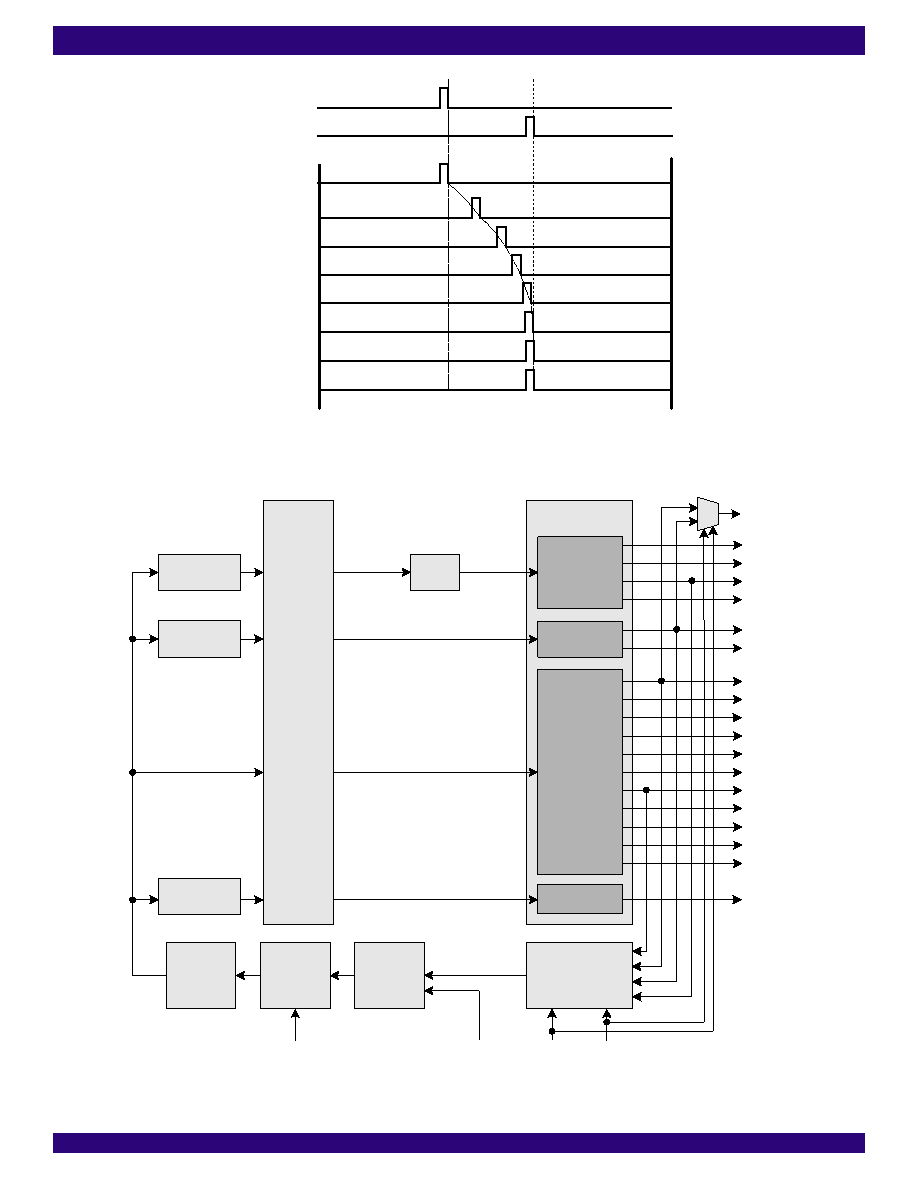
Figure - 6 Reference Switch with TIE Control Block Disabled
Figure - 7 DPLL Block Diagram
Input Clock
Ref1
Ref2
Time = 0.00 s
Time = 0.25 s
Time = 0.50 s
Time = 0.75 s
Time = 1.0 s
Time = 1.25 s
Time = 1.50 s
Time = 1.75 s
Output Clock
Di
git
al
Co
ntro
lOsc
illat
or
C32o
C16o
C8o
C4o
C2o
C3o
C6o
F0o
F8o
RSP
TSP
F16o
C1.5o
F32o
Output Interface
T1_Divider
E1_Divider
C6_Divider
Frequency
Selection Circuit
Phase
Detector
Virtual Reference
Loop Filter
Fraction_C6
Fraction_T1
24.704 MHz
32.768 MHz
25.248 MHz
Feedback Signal
Limiter
FLOCK
F_sel1
F_sel0
C19_Divider
155.52 MHz
F19o
C19o
APLL
19.44 MHz
Fraction_C19
C19NEG
C19POS
C2/C1.5
发布紧急采购,3分钟左右您将得到回复。
相关PDF资料
IDT82V3012PVG8
IC PLL WAN T1/E1/OC3 DUAL 56SSOP
IDT82V3155PVG
IC PLL WAN T1/E1/OC3 DUAL 56SSOP
IDT82V3202NLG
IC PLL WAN EBU SGL 68-VFQFPN
IDT82V3255TFG
IC PLL WAN SMC STRATUM 3 64-TQFP
IDT82V3280APFG
IC PLL WAN SE STRATUM 2 100TQFP
IDT82V3285AEQG
IC PLL WAN SE STRATUM 100TQFP
IDT82V3285EQG
IC PLL WAN SE STRATUM 100TQFP
IDT82V3288BCG
IC PLL WAN 3E STRATUM 2 208CABGA
相关代理商/技术参数
IDT82V3011PVG8
功能描述:IC PLL WAN T1/E1/OC3 SGL 56-SSOP RoHS:是 类别:集成电路 (IC) >> 时钟/计时 - 专用 系列:- 标准包装:1,500 系列:- 类型:时钟缓冲器/驱动器 PLL:是 主要目的:- 输入:- 输出:- 电路数:- 比率 - 输入:输出:- 差分 - 输入:输出:- 频率 - 最大:- 电源电压:3.3V 工作温度:0°C ~ 70°C 安装类型:表面贴装 封装/外壳:28-SSOP(0.209",5.30mm 宽) 供应商设备封装:28-SSOP 包装:带卷 (TR) 其它名称:93786AFT
IDT82V3012
制造商:IDT 制造商全称:Integrated Device Technology 功能描述:T1/E1/OC3 WAN PLL WITH DUAL REFERENCE INPUTS
IDT82V3012PV
制造商:Integrated Device Technology Inc 功能描述:
IDT82V3012PVG
功能描述:IC PLL WAN T1/E1/OC3 DUAL 56SSOP RoHS:是 类别:集成电路 (IC) >> 时钟/计时 - 专用 系列:- 标准包装:1 系列:- 类型:时钟/频率发生器,多路复用器 PLL:是 主要目的:存储器,RDRAM 输入:晶体 输出:LVCMOS 电路数:1 比率 - 输入:输出:1:2 差分 - 输入:输出:无/是 频率 - 最大:400MHz 电源电压:3 V ~ 3.6 V 工作温度:0°C ~ 85°C 安装类型:表面贴装 封装/外壳:16-TSSOP(0.173",4.40mm 宽) 供应商设备封装:16-TSSOP 包装:Digi-Reel® 其它名称:296-6719-6
IDT82V3012PVG8
功能描述:IC PLL WAN T1/E1/OC3 DUAL 56SSOP RoHS:是 类别:集成电路 (IC) >> 时钟/计时 - 专用 系列:- 标准包装:1,500 系列:- 类型:时钟缓冲器/驱动器 PLL:是 主要目的:- 输入:- 输出:- 电路数:- 比率 - 输入:输出:- 差分 - 输入:输出:- 频率 - 最大:- 电源电压:3.3V 工作温度:0°C ~ 70°C 安装类型:表面贴装 封装/外壳:28-SSOP(0.209",5.30mm 宽) 供应商设备封装:28-SSOP 包装:带卷 (TR) 其它名称:93786AFT
IDT82V3155
制造商:IDT 制造商全称:Integrated Device Technology 功能描述:ENHANCED T1/E1/OC3 WAN PLL WITH DUAL REFERENCE INPUTS
IDT82V3155PV
制造商:IDT 制造商全称:Integrated Device Technology 功能描述:ENHANCED T1/E1/OC3 WAN PLL WITH DUAL REFERENCE INPUTS
IDT82V3155PVG
功能描述:IC PLL WAN T1/E1/OC3 DUAL 56SSOP RoHS:是 类别:集成电路 (IC) >> 时钟/计时 - 专用 系列:- 标准包装:1,500 系列:- 类型:时钟缓冲器/驱动器 PLL:是 主要目的:- 输入:- 输出:- 电路数:- 比率 - 输入:输出:- 差分 - 输入:输出:- 频率 - 最大:- 电源电压:3.3V 工作温度:0°C ~ 70°C 安装类型:表面贴装 封装/外壳:28-SSOP(0.209",5.30mm 宽) 供应商设备封装:28-SSOP 包装:带卷 (TR) 其它名称:93786AFT